|
A. Coherent and THz Photonics
Profs.
Ci-Ling Pan, Ru-Pin Chao Pan, Jung Y. Huang, Gong-Ru Lin and
Jin-Wei Hsu
Major research outcomes in this area include generation of
sub-single-cycle optical pulses, adaptic coherent control,
dipole antennas with detection bandwidth exceeding 30 THz,
a record for ion-implanted photoconductors (OptExp’04,
selected by the AIP virtual journal), first
directly-modulated THz communication link for audio and
burst signals (Opt Exp’05). Prof. Pans’ group also pioneered
the field of Liquid Crystal THz Photonics, achieving the
first room-temperature, 0-2p
tunable THz phase shifter [OptExp04, selected by the AIP
Virtual Journal, Taiwan Patent 200186, US patent pending],
an important milestone for THz phased array applications.
The work on other liquid-crystal-enabled THz functional
devices such as a tunable THz Lyot filter (APL’06,
Taiwan and U.S.
patents pending) was highlighted by SPIE Newsroom
(http://spie.org/x14608.xml).
In collaboration with ITRI, the NCTU team has developed a
THz System for Detecting of biological tissue burn trauma (Taiwan
patent I276425,
U. S.
patent 7307258 B2). In collaboration with Prof. Jin-Wei Shi,
Prof. Pan and co-workers have developed high-speed optical
detectors and THz photonic transmitters with bandwidth
beyond several hundred GHz (APL’06, PTL’07, PTL’08). In
collaboration with Prof. Chi-Kuang Sun (NTU), we have
reported low-loss hollow-core THz fiber wave guide [APL’08,
highlighted by Nature Photonics, April 2008].
Scanning and interferometric THz fiber endoscopic
imaging was also demonstrated (APL’08, OptExp’08).
1.
Ultrabroad band THz field detector based on
Arsenic-ion-implanted GaAs and proton-bombarded InP (Prof.
Ci-Ling Pan):
A detection bandwidth exceeding 30 THz was reported for THz
dipole antenna fabricated on InP:H+ [Opt. Exp.
12(13):2954, 2004,
selected by the Virtual J. of Ultrafast Sci., August 2004].
This is an extension of our previous work on
Arsenic-ion-implanted GaAs [APL 83(7)1322, 2003,
selected by the
Virtual J. of Ultrafast Sci., September, 2003].
Both types of devices exhibit the broadest bandwidth
reported for THz antennas based on ion-implanted
photoconductors and comparable to that of LT-GaAs, the
current state-of-art material for such applications. A
photoconductive THz Spiral Antenna fabricated on
multi-Energy Arsenic-Ion-Implanted GaAs also was
well-received [JAP 98:013711, 2005.
Selected by the
Virtual J. of Ultrafast Sci., August 2005]. Such
antennas were used for the first directly-modulated THz
communication link for audio and burst signals (Opt Exp 13,
10416-10423, 2005) In collaboration with ITRI, the NCTU team
has developed a THz System for Detecting of biological
tissue burn trauma (Taiwan patent I276425, U. S. patent
7307258 B2).


2.
Novel
Photonic THz Transmitters (Profs. Jin-Wei Shi and Ci-Ling
Pan)A
detection bandwidth exceeding
We have
investigated two types of sub-THz Photonic-Transmitters.
The first design is based on
Separated-Transport-Recombination Photodiodes (STR-PD) based
on low-temperature MBE-grown GaAs (LTG-GaAs) and a
Micromachined Slot Antenna [PTL 19:840, 2007].
Under femtosecond optical pulse illumination, this
device radiates strong electrical pulses (4.5-mW peak power)
without the use of a Si-lens.
The peak power is as
high as 300
mW,
occuring at 500 GHz, which corresponds to the designed
resonant frequency of the slot antenna. The saturation
problem related to the output terahertz power that occurs
with the traditional LTG-GaAs-based photonic-transmitters
when operated under high external applied electrical fields
( 50 kV/cm) has been eliminated by the use of our device.

An
alternative design, appropriate for wireless THz
impulse-radio (IR) communication, is realized by monolithic
integration of a GaAs/AlGaAs based uni-traveling-carrier
(UTC) photodiode with a substrate-removed broadband antenna.
The device can radiate strong sub-THz pulses (20mW
peak-power) with a narrow pulse-width (<2ps) and wide
bandwidth (100~250GHz).
The maximum average power emitted by our device,
under the same THz time-domain spectroscopic setup, is
around 10 times higher than that of the
low-temperature-grown GaAs based photoconductive antenna,
whilst with a much lower DC bias (9V vs. 35V). [PTL, to
appear 2008].

3.
Liquid
crystal THz photonics (Prof. Ci-Ling Pan and Ru-Pin Pan)
We have pioneered this field.
The optical constants of several important liquid
crystals were determined in the THz regime for the first
time [Appl.
Opt.,
42(13):
2372, 2003 and J. Biological Phys.
29(2-3):335,
2003, J. Appl. Phys.
103: 101809, 2008,
Ferroelectrics, to appear 2008].
Unexpected large birefringence was observed for the liquid
crystals 5CB and E7 in
the nematic phase. These properties were utilized to
demonstrate both magnetically and electrically controlled
THz phase shifters
[APL
83(22): 4497, 2003;
IEEE MWCL 14(2):77, 2004,], culminating in
the first
room-temperature, 0-2p
tunable THz phase shifter
[Opt.
Exp.
12(12): 2625, 2004, Selected by
the Virtual J.
Ultrafast Sci.,
September 2004,
Taiwan Patent 200186, US patent filed].
The device operates at room temperature, as opposed to
previous devices needing liquid N2 for cooling
and achieving phase shift of a few degrees at best.
Important applications such as THz phased arrayed radar
would be possible.
Recently, we also reported control of enhanced THz
transmission through 2-D metallic hole arrays using
magnetically controlled birefringence in a nematic liquid
crystal cell.
[Opt. Exp.
13(11): 3921, 2005, collected by the Nanostructured Surfaces
Web]. The first ever
THz Lyot filter [APL
88:101107, 2006, collected by
the Virtual J. of THz
Sci. and Technol.],
electrically switchable THz quarter-wave plate
[OL
31(8):1112, 2006, collected by
the Virtual J. of THz
Science and Technology, OSA
Virtual J. Biomed.
Opt.] and electrically tunable room-temperature 2p
Liquid Crystal Terahertz Phase Shifter [IEEE PTL 18(14):
1488, July 15, 2006, collected by
Virtual J. of THz
Sci. and Technol., July 2006] were
demonstrated recently.
Our work on THz photonic elements with
liquid-crystal-enabled functionalities was highlighted by
SPIE Newsroom (http://spie.org/x14608.xml)
in 2007. Other novel devices such as polarizers, phase
gratings, Solc birefringent filters have also been
demonstrated [OL, to appear 2008, Opt. Exp. 16(5):2995,
2008; OL, to appear 2008].

4.
Adaptive
coherent control: Technology and Applications (Profs. Jung
Y. Huang, Chuck Chao-Kuei Lee and Ci-Ling Pan)
A freezing phase concept has been proposed for
adaptive coherent control with a femtosecond pulse
shaper [JOSA
B 22:1134 (2005), selected by
the Virtual J.
Ultrafast Sci., 2005]. The operational
principle is based on a concept that the highest
peak intensity will correspond to a frozen phase
state of all spectral components involved in a
coherent optical pulse. It is fast and immune to the
noise and laser power fluctuation, and useful for a
variety of applications that require complete-field
characterization and adaptive coherent control on
the same setup. We applied the scheme to investigate
multiphoton processes in InAs quantum dot saturable
Bragg reflector (SBR, fabricated by Prof. Jen-Inn
Chyi, NCU). The optical transition of InAs quantum
dots can be revealed in the spectral phase
sensitivity plot of second harmonic signal. We also
achieved a three-time increase in image contrast on
regions with photoluminescent wavelength differing
only 18 nm by using coherent control nonlinear
optical microscopy.
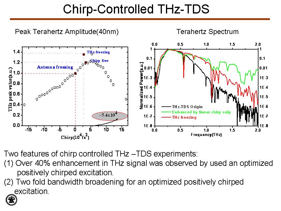
Emplying
the freezing phase algorithm, we also investigated the
enhancement of broadband THz radiation using femtosecond
pulse shaping. Over
60% radiation enhancement in output power and two-fold
broadening of bandwidth were found for optimized positively
chirped optical pulses. We
have tentatively attributed the phenomon to the increasing
saturation fluences from competition between band-filling
and pump-dump processes during excitation.
In addition, pump
power dependence of THz radiation and enhancement factor,
which is defined as ratio of peak amplitude of the radiated
THz pulse before and after adaptive control.
With fixed probe
beam power while reducing the pump power from 45mW to 5mW,
we observed an increase in the enhancement factor from 40%
to 60%. A model of
enhancement based on higher saturation flurence for
positively-chirped optical excitation is proposed.
Other factors such
as difference in absorption by leading waves in for positive
or negative chirped pulse could also contribute to the
observed phenomenon [CLEO’08, Opt. Exp., submitted, 2008].
5.
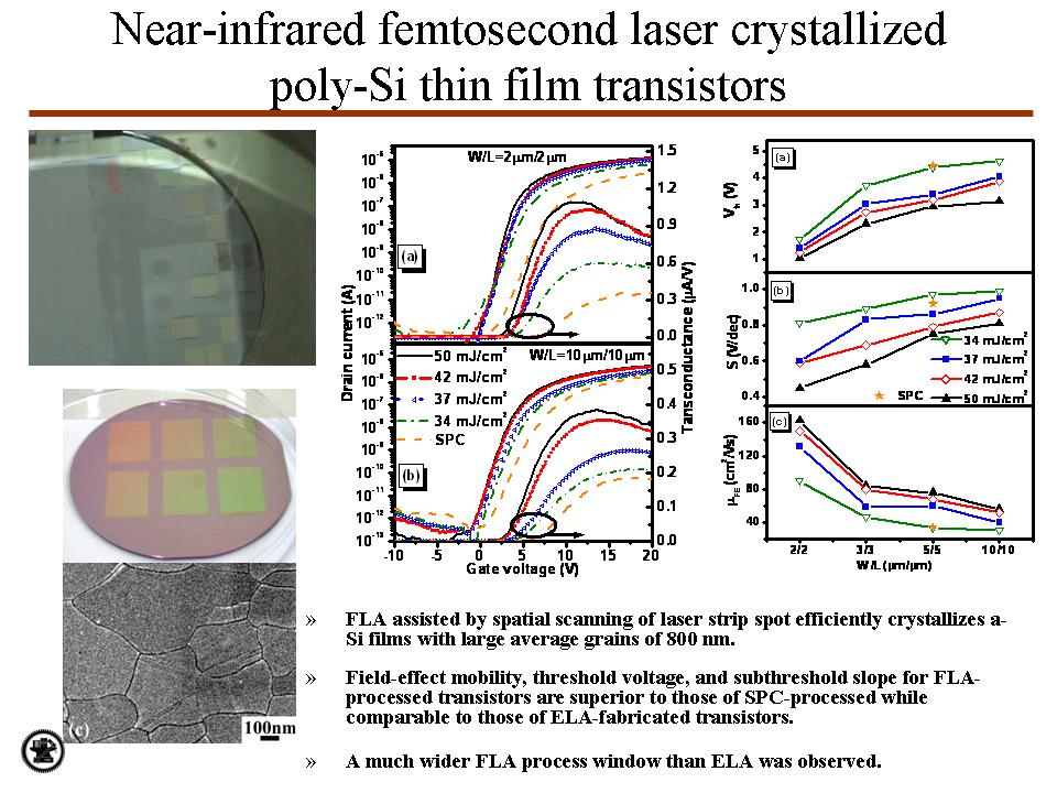
Femtosecond
LaserAnnealing: A novel approach for dopant profile
engineering and fabrication of poly-Si TFT (Prof. Ci-Ling
Pan)
Amorphous silicon (a-Si) for TFT applications was
crystallized by femtosecond laser annealing (FLA) using a
near-infrared (800 nm) ultrafast Ti:sapphire laser system
for the first time.
We found that FLA assisted by spatial scanning of
laser strip spot can crystallize a-Si films with largest
grains of ~800 nm, requiring laser fluence as low as ~45 mJ/cm2,
and low laser shots. Moreover, the optimal annealing
conditions are observed with a significant laser-fluence
window (~30%) [reported at CLEO2003 as a news story; APL
85(7):1232, 2004, selected by the Virtual J. Ultrafast Sci.,
September 2004, ROC patent I245321]. We also demonstrated
dopant profile engineering by near-infrared femtosecond
laser activation [APL 88:1311104, March 27, 2006, selected
by Virtual J. of Nanoscale Sci. and Technology, Vol. 13, No.
14, April 10, 2006 and Virtual Journal of Ultrafast Science,
Vol. 5, No. 4, April 2006]. Preamorphizing implantation is
not required. We find dopant profiles in FLA-activated
samples essentially duplicate those of as-implanted ones
even for junctions as deep as 100 nm below the surface.
Laser-recrystallized material was used successfully for
fabricating thin film transitors [Opt.
Exp., 15: 6981, 2007,
selected by
Virtual J. of Ultrafast Sci., July 2007].
THz spectroscopic techniques were employed for diagnostics
of the fs-laser-annealed poly-Si material [Photonics Asia,
invited talk, 2007, Opt. Exp. Submitted, 2008].
It is shown that The transient mobilities of poly-Si with
large (~ 500 nm) and small (~ 50 nm) grain sizes, fitted by
the Drude model, are 175.0±19.4 cm2/V s
and 94.5±20.2 cm2/V s,
respectively. We proposed that higher mobility in
large-grain poly-Si by femtosecond laser annealing is due to
reduction of deep state density rather than tail state
density.
6.
Tunable Lasers
and Electro-Optic Devices
for DWDM and
Attosecond Generation with Liquid Crystal (LC) Enabled
Functionalities and other applications (Profs. Ci-Ling Pan,
Ru-Pin Pan, Andy H. Kung):
A digitally tunable laser diode, of which the output
can be switched between wavelengths of the ITU grid
(100 GHz channel spacing) for DWDM optical
communication systems (l
= 1550 nm), is demonstrated [Optics Express,
12 (26):6434, 2004; invited talk and paper at
Photonics West 2002;
Taiwan
Patent I223484,
US
patent filed]. Another design allows continuous,
mode-hop-free electronic tuning of the laser
frequency over 20 GHz [Opt. Eng. 43(1):234, 2004; OL
29(5):510, 2004].
Dynamic wavelength switching and selection were
achieved with a liquid crystal pixel mirror (LCPM).
Fine tuning is achieved through an intra-cavity LC
phase shifter.
As an application, we recently reported intra-cavity
LC cell gap measurement [Opt. Exp. 13(20):1905,
2005].
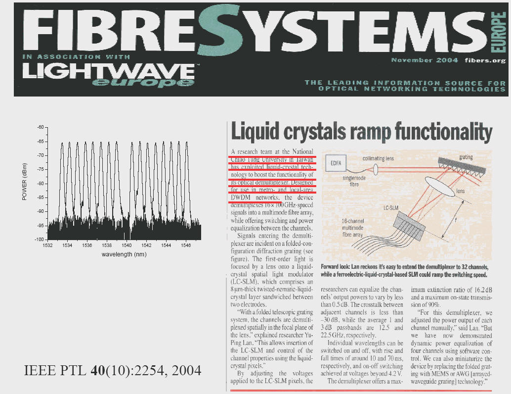
This design concept has been extended to devices such
as tunable optical switches/ filters/ equalizers/
demultiplexers. Demultiplexing 16-channel 100-GHz
-spaced signals into a 62.5-mm
multimode-fiber array was demonstrated. The central
wavelength of each channel was designed according to
the 100-GHz ITU grid. Adjacent channel crosstalk is
less than 30 dB. The outputs of the channels are
equalized to 65 dBm. The variation between different
channels reduced from 10 dB to less than 0.5 dB
[IEEE Photon. Technol. Lett.,
40(10):2254, 2004, ROC patent disclosed, 2006]. This
work was reported by Lightwave Europe in the
November issue, 2004. Recently, we report automatic
power equalization and stabilization with minimum
ripple level of a single channel down to 0.05 dB
[Opt. Comm. 278:329, 2007].
A specially designed SLM was developed and used in frequency
synthesis of attosecond pulses, in collaboration with Prof.
Andy H. Kung [Phys.
Rev. Lett. 100: 163906, 2008].
Using 7 Raman sidebands generated by molecular
modulation in H2, we achievd the synthesis of
periodic waveforms consisting of a train of pulses that are
0.83 cycles long and have an electric field pulse width of
0.44 fs.

The SLM
composed of a row of five 14 mm high by
4 mm wide by 0.022 mm thick liquid-crystal
panels. The size and location of each panel is designed to
match the sideband beam size and to allow unimpeded passage
of five sidebands. With this new modulator, a total of 7
sidebands can now be employed for waveform synthesis. The
total bandwidth is 24931.2 cm-1 or 2
octaves.
We verify by optical correlation that the carrier-envelope
phase is constant in these waveforms when they are
synthesized from commensurate sidebands. The estimated
overall shift of the carrier-envelope phase is less than
0.18 cycles from the first to the last pulse of nearly 106
pulses in the pulse train.
7.
Generation of coherent mid- and far- infrared
radiation in GaSe (Profs. Ci-Ling Pan and Jung Y. Huang)
A table-top infrared light source with high intensity and
wide tunability is constructed by use of
difference-frequency-mixing in GaSe nonlinear optical
crystal. Tuning wavelengths from 2.4μm to 28μm are obtained
with highest energy output ~13μJ at 3.5μm. The output
characteristics are compared among pure and erbium doped
crystals. Second-order nonlinear coefficient deff(2)
of the Er:GaSe crystals reveal a deff(2)
of 55.3 pm/V, which is about 24% larger than that of pure
GaSe. The improvement of deff(2) can
be attributed to the substitutive and interstitial doping of
Er ion in GaSe unit cell. [Opt.
Exp. 14:5484, 2006, selected by
Virtual J. of
Ultrafast Sci., August 2006) and Virtual J. of Biomed. Opt.].
We also report a study of the effect of optical absorption
on generation of coherent infrared radiation from mid-IR to
THz region from GaSe crystal. The infrared-active modes of
e-GaSe
crystal at 236 cm-1
and 214 cm-1
were found to be responsible for the observed optical
dispersion and infrared absorption edge. Based upon phase
matching characteristics of GaSe for difference-frequency
generation (DFG), new Sellmeier equations of GaSe were
proposed. The output THz power variation with wavelength can
be properly explained with a decrease of parametric gain and
the spectral profile of absorption coefficient of GaSe. The
adverse effect of infrared absorption on (DFG) process can
partially be compensated by doping GaSe crystal with erbium
ions. [Opt. Exp.
14:10636, 2006, selected by
Virtual J. of
Ultrafast Sci., January 2007, listed in
Virtual J. of THz
Sci. and Technol., October 2006].
Recently, we
proposed and demonstrated coherent generation and spectral
synthesis of terahertz radiation with multiple stages of
optical rectification [Opt. Exp., submitted, 2008]. This
approach can potentially be useful for the generation of
single-cycle high-amplitude terahertz pulses, which is
currently limited by the pulse walk-off effect from group
velocity mismatch.

8.
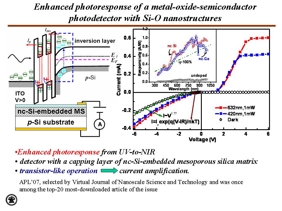
Nonlinear optical studies of Silicon nanocrystals
and Nano-Silicon-based optoelectronics (Profs. Jung Y.
Huang, Ci-Ling Pan, and Dr. Jia-Min Shieh)
A novel material of Si nanocrystals embedded in a
three-dimensional array of mesoporous silica matrix has been
studied by nonlinear optical techniques. We report
sum-frequency generation spectroscopic studies of Si-O polar
nanostructures embedded in a three dimensional array of
mesoporous silica (MS) matrix by use of different frequency
combinations with picosecond and femtosecond configurations.
Such unique electronic structure of Si nanocrystals (nc-Si)
embedded in SiO2 is opening up wide applications
to flash memory and photonic devices. The effective
second-order nonlinear coefficient and Curie temperature of
nc-Si are determined by surface sum frequency generation
spectroscopy. A resonance feature around 480 nm was
observed. The effective second-order nonlinear coefficient
is estimated to be deff =3.7 pm/V. Nonlinearity
is tentatively attributed to Si-O nanostructures in this
novel material.
The effect of heating and cooling cycle on SFG signals
provides evidence of ferroelectricity for nc-Si embedded
mesoporous silica. The Curie temperature of the material is
estimated to be 567K.

A two-terminal metal-oxide-semiconductor photodetector for
which light is absorbed in the nano-Si material described
above as a capping layer on p-type silicon substrates was
fabricated. Operated
at reverse bias, enhanced photoresponse from 300 to 700 nm
was observed. The highest optoelectronic conversion
efficiency is as high as 200%.
The enhancements
were explained by a transistorlike mechanism, in which the
inversion layer acts as the emitter and trapped positive
charges in the mesoporous dielectric layer assist carrier
injection from the inversion layer to the contact, such that
the primary photocurrent could be amplified [APL 90: 051105
2007, selected by
Virtural J. Nanoscale Sci. & Technol.2007].
This paper was at one time among the top 20 most
downloaded papers for the APL issue..
9.
Femtosecond Fiber Lasers and Applications (Profs.
Gong-Ru Lin and Ci-Ling Pan)
9-1
Self-Steepening of Prechirped Amplified
and Compressed 29-fs Fiber Laser Pulse in Large-Mode-Area
Erbium-Doped Fiber Amplifier
Prechirped amplification, soliton compression, and
self-pulse-steepening of a 300-fs stretch-pulse mode-locked
erbium-doped fiber laser (EDFL) pulse in an ultrashort
length large-mode-area erbium-doped fiber amplifier
(LMA-EDFA) and large-effect-area fiber (LEAF) link are
investigated. In situ amplified compression of the
single-mode-fiber prechirped EDFL pulse (broadened to 1.2 ps)
is initiated in the LMA-EDFA at a pumping power of
>
160
mW, which provides a 20-fold pulsewidth compressing ratio
for the incoming EDFL pulse and supports a maximum output
power of > 20
dBm. With an extremely short LEAF-based fifth-order soliton
stage, the amplified EDFL pulse can further be compressed
down to a pulsewidth of 29 fs, which gives rise to a total
pulsewidth-compressing ratio of as high as 40. The
LMA-EDFA-based prechirped and amplified soliton compression
leaves a small pedestal on the EDFL pulse with an energy
confinement ratio of 74%, providing a 20-dB magnified pulse
energy of 2.3 nJ and a 10-dB spectral linewidth of 150 nm.
The self-steepening-induced blue-side spectral
stretch by 1.3 THz is elucidated.
|
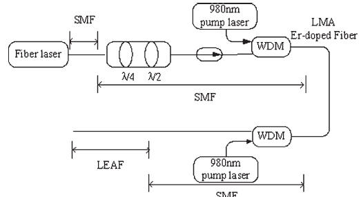
Fig. 1. Experimental setup of an LMA-EDFA
+
LEAF amplified compressor link.
|
Fig. 2. Autocorrelation traces of the
in situ
amplified and compressed
APM-EDFL pulses measured at different LMA-EDFA
output powers.
|
9-2
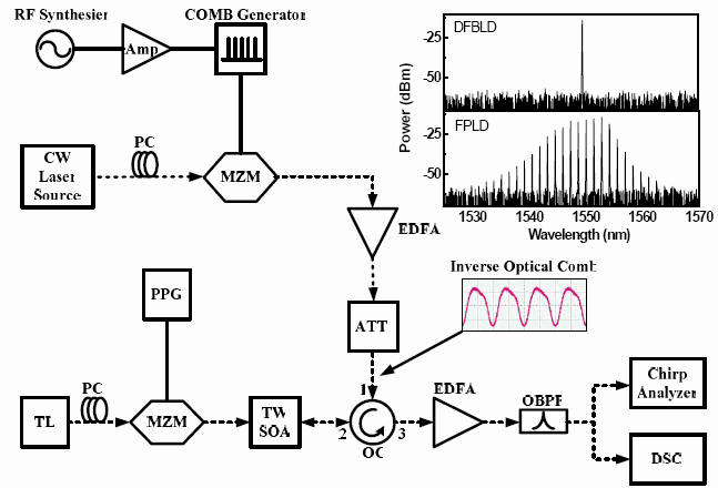
Dynamic chirp control of all-optical
format-converted pulsed data from a multi-wavelength
inverse-optical-comb injected semiconductor optical
amplifier
By spectrally and temporally reshaping the gain-window of a
traveling-wave semiconductor optical amplifier (TWSOA) with
a backward injected multi- or single-wavelength
inverse-optical-comb, we theoretically and experimentally
investigate the dynamic frequency chirp of the all-optical
10GBit/s Return-to-Zero (RZ) data-stream format-converted
from the TWSOA under strong cross-gain depletion scheme. The
multi-wavelength inverse-optical-comb injection effectively
depletes the TWSOA gain spectrally and temporally, remaining
a narrow gain-window and a reduced spectral linewidth and
provide a converted RZ data with a smaller peak-to-peak
frequency chirp of 6.7 GHz. Even at high
inverse-optical-comb injection power and highly biased
current condition for improving the operational bit-rate,
the chirp of the multi-wavelength-injection converted RZ
pulse is still 2.1-GHz smaller than that obtained by using
single-wavelength injection at a cost of slight pulsewidth
broadening by 1 ps.
|
Fig. 3. Experimental setup. Amp.: amplifier.; ATT.:
optical attenuator; DSO: digital sampling
oscilloscope; EDFA: erbium doped fibre amplifier;
OBPF: optical band-pass filter; OC: optical
circulator; PC: polarization controller; PPG: PRBS
pattern generator; TL: tunable laser. Electrical
path: solid line. Optical path: dash line.
|
Fig. 4. BER performance of the back-to-back NRZ
(blue circle) and the TWSOA converted RZ under DFBLD
(black square) and FPLD (red diamond) based
inverse-optical-comb injection.
|
9-3
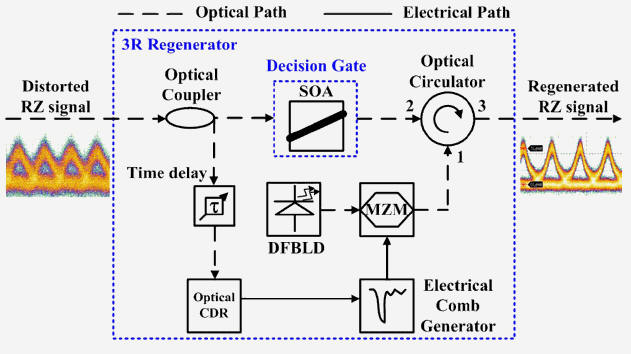
All-Optical Decision-Gating of 10-Gb/s RZ Data
in a Semiconductor Optical Amplifier Temporally Gain-Shaped
With Dark-Optical-Comb
We demonstrate a novel all-optical noninverted OC-192
return-to-zero (RZ) decision-gate by using a semiconductor
optical amplifier (SOA) which is gain-controlled to achieve
an extremely high cross-gain-modulation depth and a narrow
gain window. A dark-optical-comb generated by reshaping the
optical clock RZ data in a Mach–Zehnder intensity modulator
is employed as an injecting source to temporally deplete
most of the gain in the SOA. Such a dark-optical-comb
injected SOA decision-gate exhibits improved 3R regeneration
performances such as a timing tolerance of 33.5 ps, a
Q-factor
of 8.1, an input dynamical tolerance of 14 dB, and an
extinction ratio (ER) of 14 dB. The deviation between the
wavelengths of backward injected dark-optical-comb and input
RZ data for optimizing the ER of the decision-gate is
determined as
Δλ
= 19
nm. Under a threshold operating dark-optical-comb power of 7
dBm, such a decision-gate can recover the
−18.5-dBm
degraded RZ data with a bit-error-rate of less than
10−9
at 10 Gb/s. A negative power penalty of
−4.2
dB is demonstrated for the RZ data after 50-km propagation
and decision gating.
|
Fig. 5. Schematic diagram of the backward
optical-comb injection SOA-based decision-gate.
|
Fig. 6. (Top) Distorted RZ data-stream with “11010”
pattern at 10 Gb/s.(Bottom) Converted data stream.
|
9-4
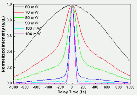
Simultaneous pulse amplification and
compression in all-fiber-integrated pre-chirped
large-mode-area Er-doped fiber amplifier
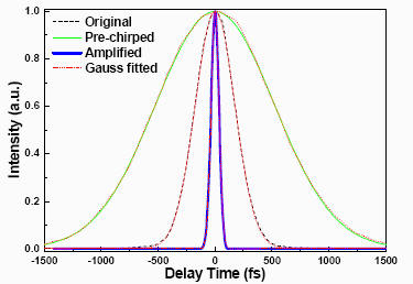
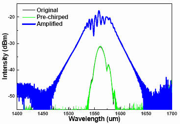
A large-mode-area Erbium-doped fiber amplifier (LMA-EDFA)
based all-fiber-integrated amplified compressor with
ultrashort length of 5.37 m and ultralow pumping power (260 mW) is proposed.
The LMAEDFA suppresses nonlinear
soliton-self-frequency-shift effect happened during
femtosecond pulse amplification, in which the fiber laser
pulse is reshaped to a low-pedestal hyperbolic-second shape
with nearly 100% energy confinement. The pre-chirped
amplification from 0.96 to 104 mW and the simultaneous
compression of a passively mode-locked fiber laser pulse
from 300 to 56 fs is demonstrated. The input pulse energy of
24 pJ is amplified up to 2.6 nJ with shortened pulsewidth of
56 fs and peak power as high as 46 kW.
|
Fig. 7. Autocorrelation traces (left) and
corresponding pulse spectra (right) of the original,
the pre-chirped and the amplified/compressed pulses.
|
9-5
Femtosecond mode-locked Erbium-doped fiber
ring laser with intra-cavity loss controlled full L-band
wavelength tunability
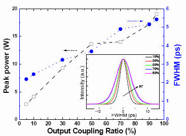
By using a tunable-ratio optical coupler (TROC) to adjust
the wavelength dependent intra-cavity loss, a L-band
mode-locked erbium-doped fiber-ring laser (ML-EDFL) is
demonstrated for generating wavelength-tunable femtosecond
pulses. The change of output coupling ratio introduces
different intra-cavity loss and shifts the peak of
mode-locked gain profile to provide continuous detuning on
wavelength of the ML-EDFL. A maximum tuning range of about
40 nm (from 1565.1 to 1605.3 nm) by decreasing the output
coupling ratio from 95% to 5% is obtained, corresponding to
a wavelength tuning slope of 2.25 nm/dB. The ML-EDFL
exhibits a super-mode suppressing ratio as high as 47 dB and
a pulsewidth of <5 ps at repetition frequency of 1 GHz.
Nearly transform-limited pulsewidth of 580 fs is generated
by linear dispersion compressing the EDFL pulses with a 32.5m-long single-mode fiber under an output
coupling ratio of 10%.
|
Fig. 8. Schematic diagram of the mode-locked EDFL
with a TROC-based wavelength tuning configuration.
Amp: microwave amplifier; COMB: electrical comb
generator; MZM: Mach-Zehnder modulator; PC:
polarization controller; RFS: radio-frequency
synthesizer; TROC: tunable-ration optical coupler;
WDM: wavelength division multiplexing coupler.
|
Fig. 9. The peak power and the pulsewidth of the
pulses as the output coupling ratio adjust from 10%
to 90%. Inset: The autocorrelation traces of the
output pulses.
|
10.
GaN-based Vertical Cavity Surface Emitting Laser and
Light Emitting Diodes
(Prof.
Hao-Chung Kuo and Tien-Chang Lu)
10-1. Study of high reflectivity mirror for blue high
quality light emitter
In this part, we develop the high reflectivity epitaxially
grown nitride mirror, usually in the form of distributed
Bragg reflector (DBR), using MOCVD epitaxy technique. The
nitride material system usually has a serious strain problem
for the epitaxy of such multi-film structure. Therefore, the
fabrication of high reflectivity mirror for blue light
emitter is a difficult topic. In this study, we have
developed a solution for the epitaxy of high-reflectivity
reflector.
A crack-free GaN/AlN DBR incorporated with GaN/AlN
superlattice (SL) layers was successfully grown on a c-plane
sapphire substrate (Figure 1(a)). We inserted three sets of
half-wave layers consisting of 5.5 periods of GaN/AlN SL
layers and GaN layer in every five pairs of the 20 pair GaN/AlN
DBR structure to suppress the crack generation. The grown
GaN/AlN DBRs with SL insertion layers showed no observable
cracks in the structure and achieved high peak reflectivity
of 97% at 399 nm with a stop band width of 14 nm(Figure
1(b)). Based on the x-ray analysis (Figure 1(c)), the
reduction in the in-plane tensile stress in the DBR
structure with insertion of SL layers could be responsible
for the suppression of crack formation and achievement of
high reflectivity.
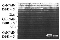 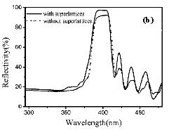
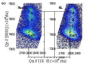
Figure 1 (a) The TEM image of GaN/AlN DBR; (b) The
reflectivity spectrum of DBRs with and without superlattice;
(c) the Reciprocal space maps
of non-SL and SL samples.
10-2. Emission characteristics of optically pumped
GaN-based vertical-cavity surface-emitting lasers
The laser emission characteristics of a GaN-based
vertical-cavity surface-emitting laser with two dielectric
distributed Bragg reflectors were investigated under
optically pumped operation at room temperature. The laser
emitted wavelength at 415.9 nm with an emission linewidth of
0.25 nm and threshold pumping energy of 270 nJ. The laser
has a high characteristic temperature of about 278 K and
high spontaneous emission coupling factor of 10−2. The laser
emission showed single and multiple spot emission patterns
with spectral and spatial variations under different pumping
conditions.
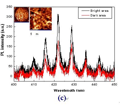 
 Figure
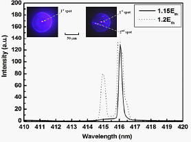
2 (a) Schematic setup of pumping and μ-PL scanning. (b)
Emission pattern of the VCSEL at pumping energy of 1.15 Eth
with single laser emission spot and 1.12 Eth with two laser
spots. The arrows indicate the position of the first and
second emission spots. Emission spectrum at pumping energy
of 1.15 Eth and 1.12 Eth, respectively. (c)
PL spectra of bright (point A) and dark (point B) areas. (d)
Laser emission intensity versus pumping energy in
semilogarithmic scale. The b value estimated from the
difference between the two dash lines is about 2x10⁻². The
inset shoes he spectrum of the laser emission with a
wavelength of 415.9nm. Figure
2 (a) Schematic setup of pumping and μ-PL scanning. (b)
Emission pattern of the VCSEL at pumping energy of 1.15 Eth
with single laser emission spot and 1.12 Eth with two laser
spots. The arrows indicate the position of the first and
second emission spots. Emission spectrum at pumping energy
of 1.15 Eth and 1.12 Eth, respectively. (c)
PL spectra of bright (point A) and dark (point B) areas. (d)
Laser emission intensity versus pumping energy in
semilogarithmic scale. The b value estimated from the
difference between the two dash lines is about 2x10⁻². The
inset shoes he spectrum of the laser emission with a
wavelength of 415.9nm.
10-3. Study of characteristics of GaN vertical cavity
surface emitting laser (VCSEL)
Following the success of laser action of GaN VCSEL using
optical pumping, we further investigated the characteristics
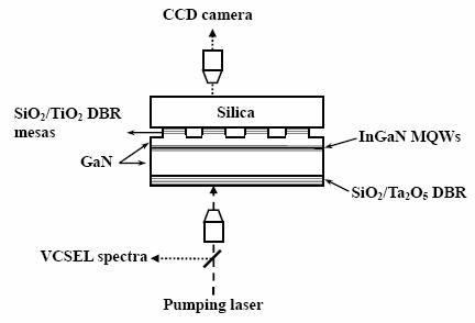
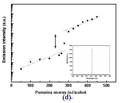
and performance of GaN blue VCSEL. The structure of GaN
VCSEL is formed by a 3λ cavity sandwiched by a 25 pairs
AlN/GaN distributed Bragg reflector (DBR) and an eight pairs
Ta2O5–SiO2 DBR (Figure 3(a)). The pumping condition could be
monitored by a CCD. The near field image was shown in figure
3(b) and laser occurred in the form of spot emission at the
center of pumping area. The GaN VCSEL emits a blue
wavelength at 448 nm with a linewidth of 0.17 nm (Figure
3(c)) with a near-field emission spot diameter of about 3μm.
The laser beam has a near linear polarization with a degree
of polarization of about 84%. The laser shows a high
spontaneous emission coupling efficiency (β) of about
5×10⁻² (Figure 3(d)) and a high characteristic
temperature of about 244 K. The high beta value also implies
the thresholdless laser for the nitride material system is
highly possible.
10-4 Successfully fabricated low-temperature electrical
pumping InGaN-MQW VCSELs by hybrid mirrors
The GaN-based VCSEL structure was grown by MOCVD (EMCORE
D-75). We use the polished
c-face (0001)
2-inch-diameter sapphire as a substrate for the epitaxial
growth. The VCSEL structure composed of
a 5λ
cavity, a 29 pairs AlN/GaN DBR as bottom mirror and an eight
pairs Ta2O5/SiO2 dielectric
mirror as the top DBR reflector. By using lithograph
technology, etching by RIE and deposed contact metals on the
substrate, we can successfully fabricate low-temperature
electrical pumping InGaN-MQW VCSELs by hybrid mirrors. The
schematic diagram of the full structure is shown in figure
4(a).
Figure 4(b) shows the photoluminescence emission intensity
as a function of wavelength at low temperature condition
(77K). From the PL spectrum, we can find the center
wavelength at 465nm and a distinct narrow linewidth of the
peak nearluy 5.2Å which can be calculated the cavity quality
factor (Q) about 894. Figure 4(c) shows the variation of
injection current with the voltage and pumping energy.
Figure 3 (a) The schematic diagram, (b) The near field
image, (c) The threshold characteristics, and (d) The beta
performance of of GaN VCSEL under optical pumping
10-4 Successfully fabricated low-temperature electrical
pumping InGaN-MQW VCSELs by hybrid mirrors
The GaN-based VCSEL structure was grown by MOCVD (EMCORE
D-75). We use the polished
c-face (0001)
2-inch-diameter sapphire as a substrate for the epitaxial
growth. The VCSEL structure composed of
a 5λ
cavity, a 29 pairs AlN/GaN DBR as bottom mirror and an eight
pairs Ta2O5/SiO2 dielectric
mirror as the top DBR reflector. By using lithograph
technology, etching by RIE and deposed contact metals on the
substrate, we can successfully fabricate low-temperature
electrical pumping InGaN-MQW VCSELs by hybrid mirrors. The
schematic diagram of the full structure is shown in figure
4(a).
Figure 4(b) shows the photoluminescence emission intensity
as a function of wavelength at low temperature condition
(77K). From the PL spectrum, we can find the center
wavelength at 465nm and a distinct narrow linewidth of the
peak nearluy 5.2Å which can be calculated the cavity quality
factor (Q) about 894. Figure 4(c) shows the variation of
injection current with the voltage and pumping energy.

Fig. 4(a). The schematic diagram of the electrical pumping
VCSEL structure. (b) The PL spectrum of the structure has
the center wavelength 465nm and a narrow linewidth 5.2A. (c) LIV
curves of the VCSEL structure has lower turn-on voltages
3.4V.
10-5 Successfully achieved the Lasing Action of
GaN-based Two Dimensional Surface-emitting Photonic Crystal
Laser
The nitride
heterostructure
in this experiment was grown by the metal-organic chemical
vapor deposition (MOCVD) system on sapphire substrate. The
epitaxial structure consists of a 25 pairs AlN/GaN DBR and a
5λ cavity.
The 2D PCSEL was fabricated by following steps. First,
200 nm Si3N4 film was
deposited
as a hard mask using PECVD and spun PMMA by spinner which
was patterned using an e-beam lithography. The lattice
constants of PCs were in the range between 180 nm and 300
nm. The diameter of each device was 50 μm. Second, the
sample was performed a dry etching in an ICP-RIE system to
etch GaN as deep as 400 nm. Finally, the sample was dipped
in BOE to remove the hard mask to complete
2D PCSEL.
Figure 5(a) and (b) show the schematic diagram of our
2D PCSEL,
and the SEM image of fabricated 2D PCSEL in top view,
respectively.
The
threshold characteristics of PCSEL were also measured.
Taking one of them for example (a = 290 nm), the
laser emission intensity from the PCSEL as a function of the
exciting energy density is shown in figure 5(c). The
threshold energy density (Eth) was observed to be
around 3.5 mJ/cm2. The light intensity increased
rapidly and linearly as the excitation energy density was
above the threshold. Figure 5(d) shows the lasing spectra at
different pumping energy. A sharp and narrow laser emission
was then clearly observed as the pumping energy increased
above the threshold energy. The lasing wavelength located at
424.3 nm, and the FWHM of the laser is around 0.11 nm. Other
devices also could be observed the lasing actions occur at
the similar threshold energy but different lasing
wavelength.

Figure 5
(a) The schematic diagram of the overall photonic crystal
surface emitting laser structure. (b) The SEM image of the
full structure in top view. (c) The light output intensity
as a function of the pumping energy density at room
temperature. The threshold energy density was about 3.5 mJ/cm2.
(d) The variation of the laser emission spectrum with
increasing the pumping energy. The laser emission wavelength
is 424.3nm with a linewidth of about 0.11nm
10-6. High Light-Extraction GaN-based Vertical LEDs With
Double Diffuse Surfaces
We have demonstrated the high light-extraction (external
quantum efficiency ~40%) 465-nm GaN-based vertical
light-emitting diodes (LEDs) employing double diffuse
surfaces. The high scattering efficiency of double diffused
surfaces could be responsible for the high light output
power. A schematic cross-section image of a GaN-based LED
with double diffuse surfaces is shown in Figure 6(a) and (b)
shows the light output power (L-I curve) of sample A, sample
B and conventional LEDs. The sample B, the LED with double
diffuse surfaces, and sample A, the LED with flat
omnidirectional reflectors, produced much higher light
output as compared with that of conventional LEDs under all
our measurement condition. The calculated external quantum
efficiency of our proposal LEDs with double diffuse surfaces
is about 40% at 20mA (l~465
nm), which could compete with structures of state of the
art.
Figure 6 (c) and (d) shows the cross-sectional transmission
electron microscope (TEM) images of sample A and sample B,
respectively. In Fig. 6(c), the top surface of p-type GaN
was quite flat, as can be seen in conventional LEDs;
however, lots of hexagonal V-shape pits was observed on
p-type GaN surface of sample B, as shown in Fig. 6(d). Fig.
6(e) is an enlarged TEM image of one hexagonal V-shape pit.
As can be seen in this figure, the hexagonal V-shape pit
originated from threading dislocations and there is a thick
dark band along the V-groove, being indicative of thickness
variation.

Figure 6 (a) Schematic cross section of a GaN-based LED with
double diffuse surfaces. (b) Output power of sample A,
sample B, and conventional LEDs measured by an
integral-sphere as a function of a forward current.
Cross-sectional transmission electron microscope (TEM)
images of (c) flat p-GaN surface (sample A) and (d)
hexagonal V-shape roughened p-GaN surface (sample B).
(e) is an enlarged TEM image of one hexagonal V-shape pit.
10 -7. Fabrication and Characterization of GaN-based
LEDs Grown on Chemical Wet-etched Patterned Sapphire
Substrates (CWE-PSS)
Characteristics of GaN-based LEDs grown on patterned
sapphire substrate fabricated by the chemical wet etching
were specifically analyzed. By chemical wet etching, the
sapphire substrate exhibited a particular
crystallography-etched facet of {1-102} R-plane with an
inclined slope as large as 57o, facilitating a significant
enhancement of the light extraction efficiency. An
improvement of epitaxial quality was also achieved on
CWE-PSS LEDs, according to device reliability testing
results.
Fig. 7(a) schematically depicts the GaN-based LED grown on
the CWE-PSS and the corresponding SEM micrograph of LED full
structure is presented in Fig. 7(b). For fabricating the
CWE-PSS, the SiO2 film with hole-patterns of 3-μm-diameter
and 3-μm-spacing was deposited onto the sapphire substrate
to serve as wet etching masks. The sapphire substrate was
then wet etched using an H3PO4-based solution at an etching
temperature of 300 oC. Fig.7 (c) and (d) show top and
cross-section side views SEM images of the pattern sapphire
substrate of etching time of 90s Fig.7 (e) and (f) show the
evolution of CWE-PSS with the increase of sapphire etching
time. With the increasing of the etching time, the total
area of C-plane will decrease due to its relative faster
etching rate than R-plane. Fig.7 (g) shows the measurement
results of output power (L-I curves) of CWE-PSS LEDs with
different sapphire etching times. According to this figure,
the optimized CWE-PSS condition was achieved on the etching
time of 90s, corresponding to an enhanced factor of 1.4.
Better reliability characteristics were also observed on the
CWE-PSS LEDs, as shown in Fig.7 (h).
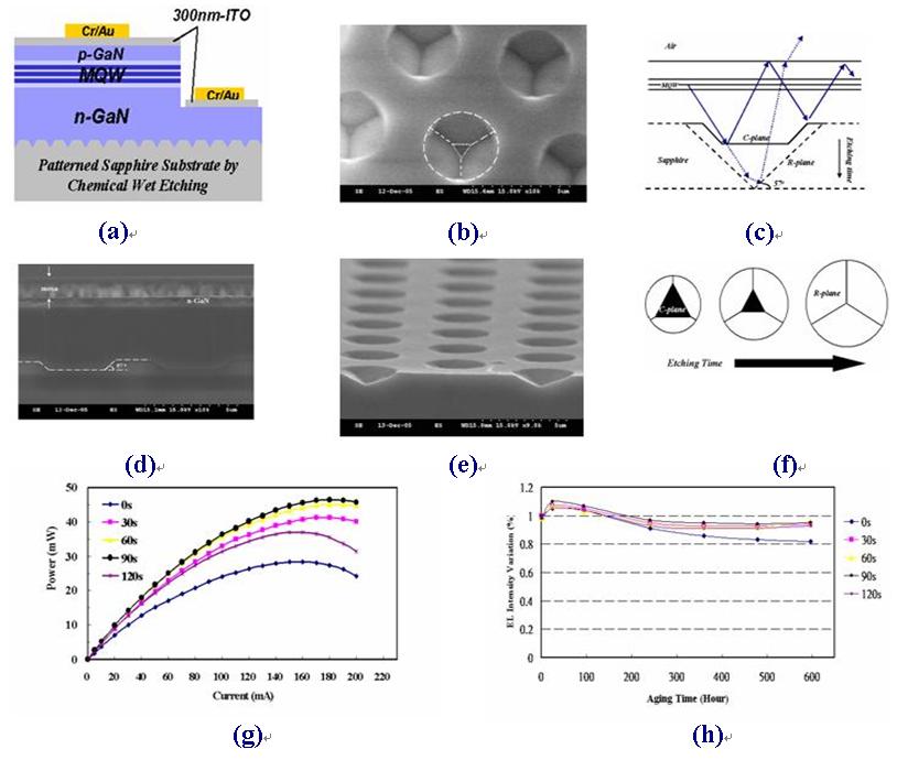
Figure 7 (a) The schematic drawing of the device structure.
(b) Cross- sectional side-view SEM images of the CWE-PSS
LEDs Structure. (c)(d) The SEM images of the top and
cross-section side views. (e)A top-view drawing depicts the
evolution of the increasing etching time. (f)A schematic
ray-tracing with increasing sapphire etching time. (g)
Output power measurement and CWE-PSS LEDs. (h) Reliability
test of the conventional and CWE-PSS LEDs under stress
condition of 55℃ and 50 mA.
10-8. Fabrication of InGaN/GaN MQW Nanorods LED by
ICP-RIE and PEC Oxidation Process with Self-Assembly Ni
Metal Islands
We successful fabricated the InGaN/GaN MQW nanorods LED
using Ni nano-masks, ICP-RIE etching and PEC oxidation
process. The PEC oxidation process can produces better
oxidation layer surrounding nanorod to isolate nanorods to
electric pumping. A transparent contact layer was deposited
to form a connection with the exposed p-type of individual
nanorod. We estimate the mean dimension and density of the
InGaN/GaN MQW nanorods LED as shown
in Fig. 8(a) which shows the SEM images of InGaN/GaN MQW
nanorods LED after ICP-RIE etching. The SEM image of in Fig.
8(b) shows the Ni/Au contact metal deposited on InGaN/GaN
MQW nanorods LED after PEC oxidation process.
Fig. 8(c) shows the normalized PL intensity spectrum of the
as-grown LED and nanorods LED with/without PEC. An
enhancement by a factor of 6/5 times in photoluminescence
intensities of nanorods with/without PEC process compared to
that of as-grown structure. The peak wavelength observed
from PL measurement shows a blue shift of 3.8 nm of the
nanorods without PEC oxidation process and 8.6 nm of the
nanorods with PEC oxidation process from that of the
as-grown LED sample. The blue shift maybe is attributed to
strain relaxation in the well for nanorods LED and intensity
enhanced by scattering effect. The Fig. 8(d) shows the
normalized EL spectrum of the as-grown LED and nanorods LED
samples with PEC process at an injection current of 1mA. The
EL spectrum shows 10.5 nm blue-shift of the nanorods with
PEC from that of the as-grown LED sample.
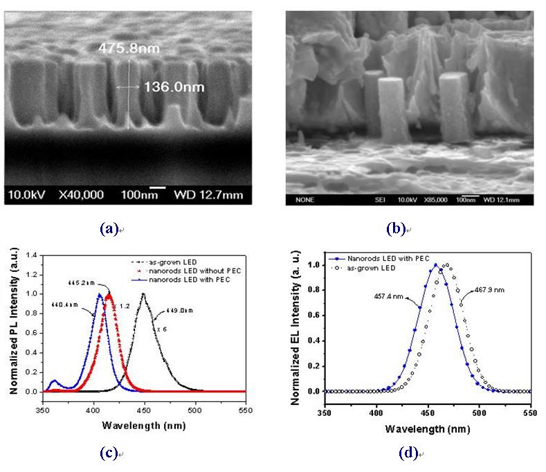
Figure 8 The SEM images of (a) InGaN/GaN MQW nanorods LED
after ICP-RIE etching. (b) InGaN/ GaN MQW nanorods LED after
deposited contact metal. (c) Normalized PL intensity spectra
for as-grown LED and nanorods LED with/without PEC
at
room temperature. (d) Normalized EL intensity spectra for
as-grown LED and nanorods LED with PEC
at
room temperature.
10-9. Study of high Q micro-cavity light emitting diode
(MCLED)
In this part, we mainly develop the micro-cavity light
emitting devices with high quality factor. The fabricated
structre of the high Q GaN-based micro-cavity light emitter
is shown in figure 9(a). It also has a similar structure
with the GaN VCSEL which is consist of a 25-pairs
high-reflectivity AlN/GaN DBR (R = 98%), a 3λ InGaN/GaN
active pn-junction
region and an 8-pairs SiO2/Ta2O5 DBR (R = 99%). The MCLED
shows that the emission intensity superlinearly increased
with a very narrow linewidth of 0.52 nm equivalents to
cavity Q value of 895 at driving current of 10 mA and a
dominant emission peak wavelength at 465.3 nm (Figure 9(c).
The quality factor is the best value compared to those
previously published value. Moreover, the MCLED also shows
an invariant emission peak wavelength with the varying
current (Figure 9(d)). It means the photon emission could be
highly control using this structure. The results should be
promising for developing a number of high performance light
emitters, including GaN-based VCSELs.
Figure 9 (a) The schematic diagram, (b) L-I-V curves, (c)
The emission spectra, and (d) The variation of wavelength of
GaN MCLED.
10-10. High-Performance GaN-based vertical-injection
light-emitting diodes with TiO2–SiO2
Omnidirectional reflector and n-GaN roughness
We have designed and fabricated a new type of GaN-based
thin-film vertical-injection light-emitting diode (LED) with
TiO2–SiO2 omnidirectional reflector
(ODR) and n-GaN roughness. The associated ODR designed for
LED operation wavelength at 455 nm was integrated with
patterned conducting channels for the purpose of vertical
current spreading. With the help of laser lift-off and
photo-electrochemical etching technologies, at a driving
current of 350 mA and with chip size of
1 mm × 1 mm, the
light–output power and the external quantum efficiency of
our thin-film LED with TiO2–SiO2 ODR
reached 330 mW and 26.7%. The result demonstrated 18% power
enhancement when compared with the results from the
thin-film LED with Al reflector replace.
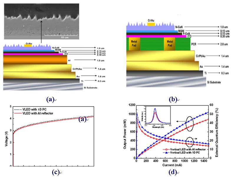
Figure 10 Schematic diagram of a VLED structure (a) with Al
mirror and roughness (b) TiO2–SiO2 ODR and
roughness. Inset in (a) shows the SEM image of surface
roughness with PEC process. (c) I–V and (d)
intensity–current (L–I) and EQE versus forward dc current
for the LED with TiO2–SiO2 ODR and roughness, and for the
LED with Al reflector and roughness fabricated in this
letter. The inset shows the room-temperature EL spectrums at
a driving current of 350 mA.
10-11. Trenched epitaxial lateral overgrowth of fast
coalesced a-plane GaN with low dislocation density
We have grown high quality and fully coalesced a-plane GaN
films at the thickness of 10 μm by using trenched epitaxial
lateral overgrowth (TELOG) with a 2 μm seed/18 μm trench
stripe pattern. Fig.1 shows the results of x-ray
measurement. The FWHMs of x-ray rocking curves along (0001) c and
(1-100) m directions were reduced from 973 to 385 arc sec
and from 1811 to 260 arc sec, respectively, demonstrating
the improvement of the crystal quality and the mitigation of
the anisotropic in-plane strains between different crystal
axes by TELOG. According to the results of μ-PL and TEM, the
TDD can be reduced largely from 1×10¹⁰ to 3×107 cm−2
for the N-face GaN wing, which was shown in Fig.2. The Ga-face
GaN could be much easily influenced by the thin GaN layer
grown on the bottom of trench, indicating that a narrower
stripped GaN seeds and deeper trench etched into the surface
of sapphire can derive a better quality a-plane TELOG GaN
film for the most of the area.
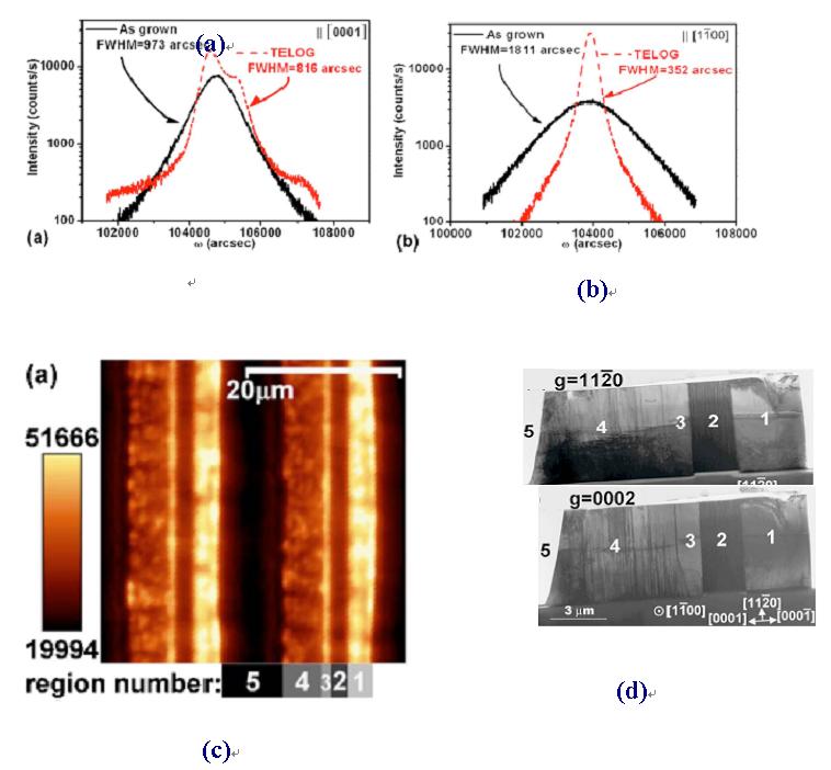
Figure 11 X-ray rocking curves of as-grown and TELOG a-plane
GaN films (a) along (0001) direction (b) along (1-100)
direction.(c) Top view μ-PL image of TELOG a-plane GaN film.
(d) and (e) Cross-sectional TEM g=(0002) and g=(11-20) two
beam bright field images.
10-12. InGaN/GaN nanostripe grown on pattern sapphire by
metal organic chemical vapor deposition
We have used MOCVD to fabricate InGaN/GaN MQWs nano-stripes
on trapezoidally patterned sapphire substrates. A series of
special relations and planes of crystallization were defined
by diffraction pattern analysis and TEM observations, which
was shown as Fig. 12. The nano-stripe structures existed on
top of the trapezoid pattern of the sapphire substrate in
zone I. In the TEM images, the MQW structures appeared only
in zones I and III. No MQW structures were detected from TEM
observation of zone II, indicating that the growth direction
might occur only toward the top and lateral facets of the
trapezoidally patterned sapphire. Fig. 12(f) shows the
results of μ-PL experiments which indicate that the
intensity of the luminescence from the MQWs embedded in the
nano-stripe structure was enhanced up to fivefold relative
to those of regular thin film MQWs, probably as a result of
much-improved internal and external quantum efficiency.
Meanwhile, dislocations that stretched from the interfaces
between the GaN and the substrates did not pass through the
MQWs in the TEM observation (Fig. 12(g)). Therefore, these
MQW nano-stripe arrays are capable of enhancing luminescence
and appear to be suitable for application to the fabrication
of high-efficiency light-emitting devices.
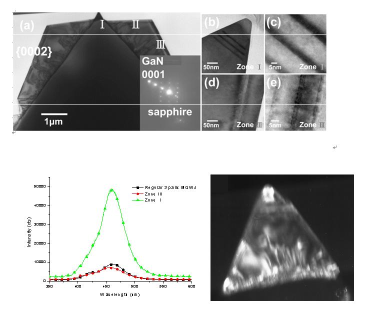
Figure 12 (a) Cross-sectional TEM image of the trapezoid
structure. The crystalline orientation between GaN and
sapphire in zone Ⅲ was defined by diffraction pattern as
shown in the inset. (b)(c) High resolution TEM images with
different magnifications of the MQWs in zone Ⅰ. (d)(e) High
resolution TEM images with different magnifications of the
MQWs in zone Ⅲ. (f) PL spectra of zone Ⅰ, zone Ⅲ and a
conventional thin film 3 pairs MQWs. (g) The cross-section
dark-field TEM images of the nano-stripe.
10-13. Enhancement of flip-chip light-emitting diodes
with Omnidirectional reflector and textured micropillar
arrays
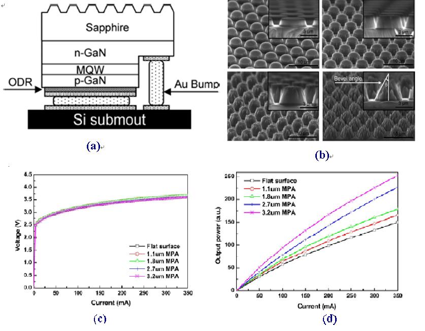
The flip-chip light-emitting diodes (FC-LEDs) with a
conductive omni-directional reflector and textured
micropillar arrays were investigated. The micropillar arrays
structure was formed on the bottom side of sapphire
substrate by dry etching process to increase the
light-extraction efficiency. Fig. 12(a) shows the schematic
diagram of FC-LEDs structure with micropillar arrays
surface. The surface morphology of the FC-LED with different
etching condition sapphire surface was examined by scanning
electron microscope as shown in Fig. 12(b). The
corresponding current–voltage (I–V
) characteristics of flat surface FC-LEDs were also
measured, respectively, as shown in Fig.12(c). The
light output power of the FC-LED was increased by 65% for a
3.2-μm
textured micropillar on the bottom side of the sapphire
substrate as shown in Fig. 12(d). Our work offers promising
potential for enhancing output powers of commercial
light-emitting devices.
10-14
Enhancement of light output intensity by integrating ZnO
nanorod arrays on GaN-based LLO vertical LEDs
Enhancement of
light output intensity for GaN-based vertical light-emitting
diodes, combining wafer bonding and the laser lift-off (LLO)
process, employing an omnidirectional extraction surface
with synthesized single-crystal ZnO nanorod arrays in
aqueous solution at room temperature is presented. Figure
13(a) to 13(d) shows the FESEM images of the synthesized ZnO
nanorods on different surfaces. Figure 13(e) shows the
current to voltage (I-V) curve of the VLED with and without
ZnO nanorods. The light output intensity and wall-plug
efficiency of the GaN-based LLO vertical LED with the
omnidirectional extraction surface by ZnO nanorod arrays
shows 38.9 and 41.2% increases, respectively, at 200
mA current injections compared to that of a vertical LED
without ZnO nanorod arrays as shown in figure 13(f). The ZnO
nanorod arrays not only support a current spreading layer
but enhance the probability of photon escape through the
omnidirectional extraction surface.

Figure 13.
FESEM images of the GaN-based LEDs with ZnO nanorod arrays:
(a) cross-sectional image of the synthesized ZnO nanorod
arrays, (b) images of the n-GaN surface, (c) images of the
bonding pad metal surface, and (d) images of the passivation
SiO2 surface. (e) I-V and (f) L-I
and WPE vs forward dc current for the GaN-based LLO LED
with ZnO nanorod arrays and that without ZnO nanorod arrays
fabricated in this letter.
11.
ctagonal
Quasi-Photonic Crystal Nanocavity Lasers with Side-Mode
Reduction and Condensed Device Size :(Po-Tsung
Lee)
 We first propose a brand new single-defect nanocavity by
using octagonal (8-fold) quasi-periodic photonic crystal
(QPC) lattice. Both in finite-difference time-domain (FDTD)
simulations and experimental measurements, we successfully
confirm the resonance and lasing of WG mode with azimuthal
number four in this nanocavity.
We first propose a brand new single-defect nanocavity by
using octagonal (8-fold) quasi-periodic photonic crystal
(QPC) lattice. Both in finite-difference time-domain (FDTD)
simulations and experimental measurements, we successfully
confirm the resonance and lasing of WG mode with azimuthal
number four in this nanocavity.
In numerical simulations, we also identify all resonance
modes in the nanocavity. We find that resonance modes are
far away from each other in frequency. This is an
advantageous property for reducing the influence of side
modes in the nanocavity, which is better than other reported
photonic crystal single-defect nanocavities.
Due to the central zero-field distribution of WG mode
profile, we successfully reduce the side mode by inserting a
central air hole in the nanocavity without affecting the WG
mode resonance. The side-mode suppression-ratio (SMSR) is
increased up to larger than 30dB. We also investigate and
discuss the possibility of electrical-driven structure based
on this WG mode.
Due to the isotropic photonic bandgap (PBG) effect of
octagonal QPC lattice, we successfully obtain the WG mode
lasing actions with very condensed device size of 3.5 μm
×
3.5 μm and low effective threshold
power of 0.2 mW. This indicates that this device can be
easily integrated into PICs without affecting other
integrated devices, which is a very important property.
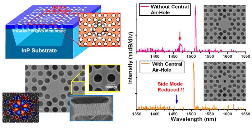
Fig. 1: (Left) The scheme of single-defect nanocavity design
and the scanning-electron microscope (SEM) pictures of
fabricated devices. (Right) The WG mode lasing actions and
its side mode reduction after inserting perturbation in the
central of the nanocavity.
12.
High
Quality Factor Dodecagonal QPC Microcavity Laser and Its
Strong Mode Dependence :
(Po-Tsung
Lee)
We propose and design a microcavity based on 12-fold QPC
lattice with well-sustained WG mode and without any cavity
modification, which is very different from octagonal QPC
single-defect nanocavity.
In numerical simulations, we successfully obtain the
well-sustained WG mode with azimuthal number six and
identify all resonance modes in the microcavity.
We obtain a very high measured quality (Q)
factor of 10,000 from well-fabricated devices.
By randomly varying the outer and inner-most lattice
positions of the microcavity, we propose and confirm a
strong WG mode dependence on nearest air holes in theory and
experiments. This is a very important conclusion and
provides us the concept for our following researches to
enhance WG mode in ordinary photonic crystal microcavities.
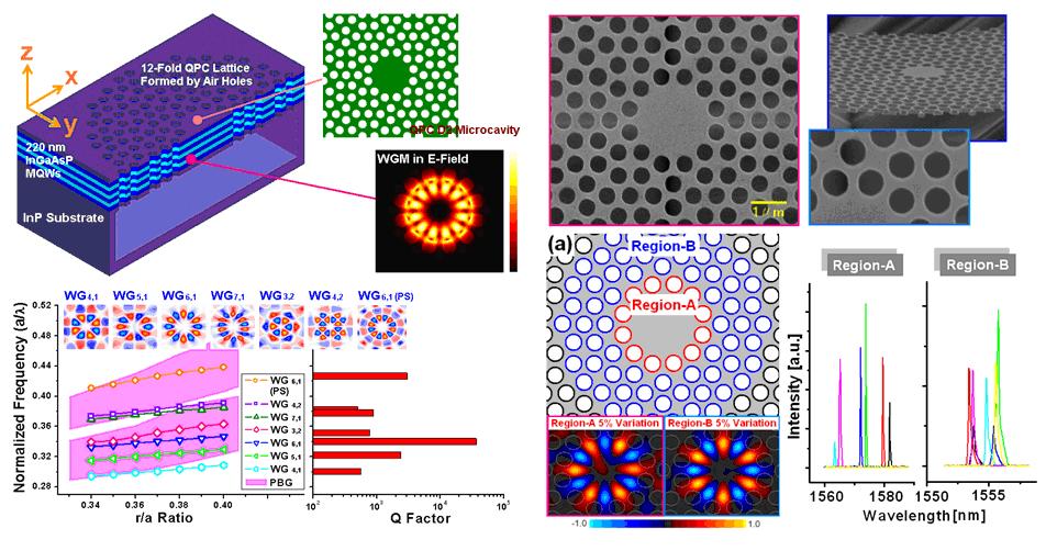
Fig. 2: (Left) The scheme of 12-fold QPC microcavity with WG
mode and the simulated resonance modes properties. (Right)
The SEM pictures of fabricated devices and its strong mode
dependence under different cavity boundary conditions.
13.
Circular
Photonic Crystal with Isotropic PBG Effect and Its High
Q
Microcavity Laser :
(Po-Tsung
Lee)
We also investigate a novel QPC lattice structure named
circular photonic crystal (CPC). By using FDTD simulations,
we successfully confirm the better PBG isotropy compared
with that of ordinary photonic crystals, including the
variations of PBG width and boundary in different lattice
directions.
Using this isotropic PBG effect, we design a CPC microcavity
with WG mode and high
Q factor. In experiments, we successfully obtain
measured Q factor
as high as 11,000 and ultra-low effective threshold power
smaller than 20 μW. It is worth to note that this is the
highest Q factor
ever reported in photonic-crystal-based microcavity by using
multiple quantum wells (MQWs). Thus, the published results
have been selected
for Virtual
Journal of Nanoscale Science & Technology in the issue of
Apr. 30, 2007.
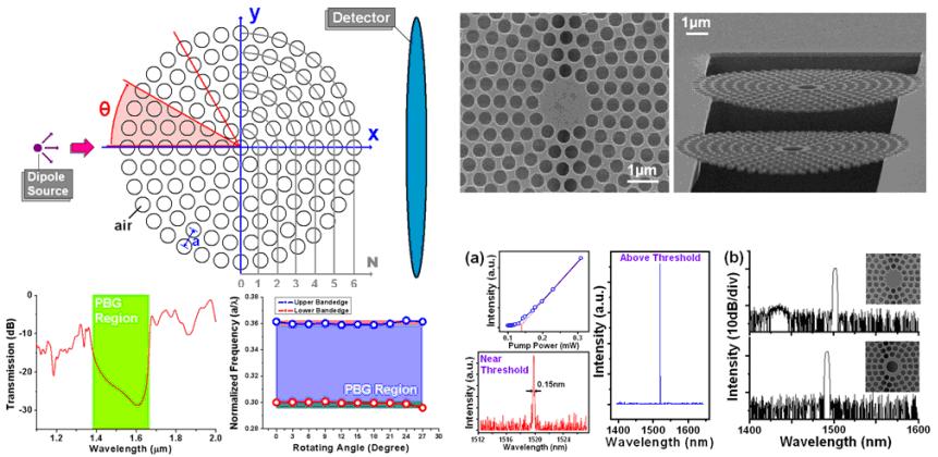
Fig. 3: (Left) The scheme of circular photonic crystal and
its isotropic photonic bandgap effect. (Right) The SEM
pictures of fabricated devices and its lasing action with
high Q factor of
11,000.
14.
Enhanced
WG Mode in Photonic Crystal Circular-Shaped Microcavity and
Its Uniform Coupling Properties in Cavity-Waveguide System :
(Po-Tsung
Lee)
We first propose the concept of combining topology and
micro-gear lasers to enhance the WG mode in a photonic
crystal microcavity by modifying the cavity boundary by
repositioning the 12 nearest air-holes around the cavity.
In numerical simulations, we successfully confirm and obtain
the existence of enhanced WG mode. We also obtain a high
measured Q factor
of 7700 from well-fabricated devices.
Both in simulations and experiments, we first investigate
the uniform photonic crystal cavity-waveguide coupling
property due to the presence of WG mode. This provides a
promising solution for serious non-uniform cavity-waveguide
coupling problems in most photonic crystal nano- and
micro-cavities.
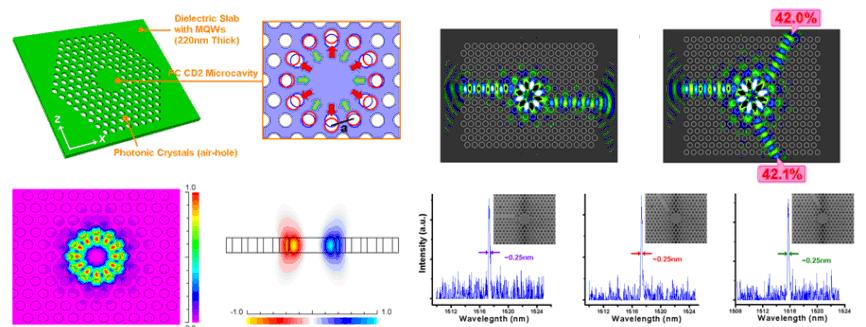
Fig. 4: (Left) The scheme of photonic crystal
circular-shaped microcavity and its enhanced WG mode.
(Right) The uniform coupling properties both in simulations
and experiments are obtained when combining the cavity with
external waveguides.
11.
Volume Holographic Data Storage(Profs.
Ken Yuh Hsu and Shiuan Huei Lin)
The main target of this project is to explore novel
materials for volume and/or dynamic holographic recording
and its applications on ultrahigh density storage (~Tbits/in2).
During the forth year of project, we have investigated on
the optimization of our doped PMMA photopolymers. In the
holographic data storage experiments, we have
fabricated a 5-inch diameter photopolymer disk with 2-mm
thickness. It was put into a shift-multiplexed holographic
data storage system (shown in Fig. 1.) and used to stored
binary data as a computer data bank. We have written ~57
holograms, at a storage density of ~ 175 bits/mm2,
corresponding to ~ 150GB of the storage capacity in this
5-inch disk. Raw bit error rate has been estimated to be
~0.0015. This result demonstrates that our material can
support for the high-quality volume holographic storage
applications. This system is suited for fundamental
investigations of the material aspects of PQ:PMMA; however,
as typical experimental setups with numerous facilities for
mechanical and optical adjustments, they are n ot
optimized in terms of system complexity. In order to improve
the commercial prospect of a holographic mass storage based
on doped photopolymers, read/write setups with reduced
system complexity and with the potential to be fabricated at
low cost are necessary. In forth year, we start to design a
particularly promising system architecture that is based on
the concept of planar-integrated free-space optics (PIFSO). ot
optimized in terms of system complexity. In order to improve
the commercial prospect of a holographic mass storage based
on doped photopolymers, read/write setups with reduced
system complexity and with the potential to be fabricated at
low cost are necessary. In forth year, we start to design a
particularly promising system architecture that is based on
the concept of planar-integrated free-space optics (PIFSO).
The idea of PIFSO is to miniaturize and “fold” a free-space
optical system with a certain desired functionality into a
transparent substrate of a few millimeters thickness in such
a way that all optical components fall onto the
plane-parallel surfaces. Passive components such as lenses
or beam deflectors can then be integrated into the surfaces,
for example, through surface relief structuring, and the
implementation as diffractive optical components offers an
almost unlimited design freedom. Active components such as
optoelectronic I/O devices can be bonded on top of the
plane-parallel substrates. Reflective coatings ensure that
optical signals propagate along zigzag paths inside the
substrate.
Since all passive components are arranged in a planar
geometry, the optical system can be fabricated as a whole
using mask-based techniques. Lithographic precision for the
lateral positioning of components is thereby ensured.
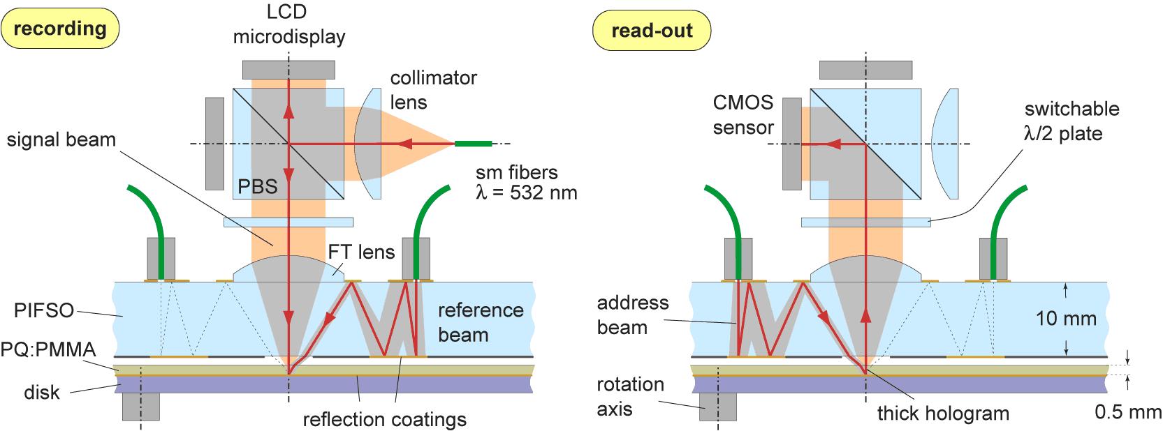
Figure
2
Schematic setup of the PIFSO-type reflection holographic
read/write system depicting it in the recording and in the
read-out mode. Reference and address beams are exactly
counterpropagating along zigzag paths inside the PIFSO
substrate. The FT lens performs an optical Fourier
transformation from the LCD and the CMOS sensor to the
PQ:PMMA layer on the storage disk.
We apply the PIFSO principle for the construction of a
read/write head for holographic storage disks. Figure 2
shows the proposed bidirectional Fourier optical system
architecture in the recording and the readout mode.
One can recognize an orthogonal signal beam, skew
reference, and address beam paths that intersect at a target
position on the reflective lower side of the photosensitive
layer of the storage disk on which the hologram is recorded.
All beams originate from the same laser source from
which they are coupled into the PIFSO system by single-mode
optical fibers.
The relay of the signal beam from the fiber end to the disk
is carried out by a 4-f system; in its Fourier plane, the
expanded beam is 2D spatially modulated by a LCD
microdisplay. To be able to record a complete signal page
without loss, the diameter of the reference beams has to be
matched to the width of the signal spectrum at the disk.
Reference and address beams are furthermore perfectly
collimated and counterpropagating so that they can be
considered as mutually phase conjugate.
Hence, if the reference beam is used for the
recording of a hologram, then a readout with the address
beam will generate the phase-conjugate version of the
original signal beam; this reconstructed beam propagates
through the 4-f system in the opposite direction and is
projected onto a CMOS sensor.
In summary, during this year a strategy using doped
photopolymers to fulfill most of the material requirements
has been proposed and demonstrated. The concept of using
planar-integrated free-space optics to realize
microintegration of the optical read/write head has been
explored. With these two innovations, we anticipate further
accelerated advances in page-oriented holographic data
storage techniques in the near future that may eventually
lead to a scientific breakthrough.
|