Recent concepts for novel spintronic devices have emerged, and theses are generating new enthusiasm for spin transistor research. More specifically, motivation for realizing robust electrical spin injection now arises from recent developments in spin transistor. The former refers the use of spin-polarized currents to achive magnetic actuation, and the latter refers to prospects for electrical control of the polarization of localized nuclear or electric moments. Both phenomena may ultimately play important roles in future spintronic systems and in the longer-term quest for realizing solid-state quantum logic.
Spin-valve
Transistor (SVT)
Consider an F1-N-F2 system,
simple band models can be used to illustrate device operation [M. Johnson,
J. Magn. Magn. Mater. 156, 321(1996)]. In the figure, a bias current Ie
is applied to F1 and N, and D represents a detector characterized
by a variable load resistance. The nonequilibrium magnetization M in N
generates an electric field at the N-F2 interface such that
the voltage across, or current through. Therefore, D is positive when
the magnetizations M1 and M2 of F1 and
F2 are parallel and is negative when M1 and M2
are antiparallel.
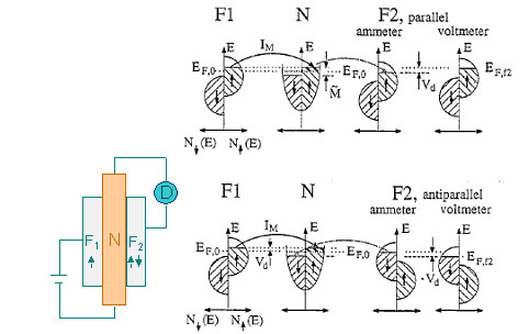
Microscopic models of electron transport, using plots of the DOS for the parallel and antiparallel configurations of the ferromagnets F1 and F2.
The perpendicular electron transport and exponential mean free path dependence in a metal base transistor allows for fundamental detection of the perpendicular spin-valve effect by incorporating a spin-valve into the base. A SVT consists of spin-valve multilayers sandwiched between two potential barriers made of two semiconductors or an insulator and a semiconductor. The emitter barrier injects hot electrons into the spin valve base and the collector current very sensitive to magnetic fields.
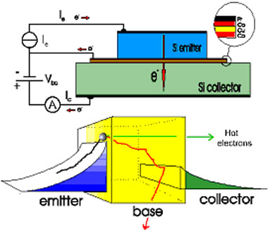
Schematic cross-section of the spin-valve transistor. A Co/Cu/Co sandwich base is sputtered on a silicon substrate. Vacuum bonding is done while sputtering the Pt layer. The picture shows the band-structure of the spin-valve transistor. [Monsma et al., Science 281, 407(1998)
A spin-valve transistor (SVT) that employs hot
electrons is shown to exhibit a huge magnetotransport effect at room
temperature in small magnetic fields. The SVT is a ferromagnet-semiconductor
hybrid structure in which hot electrons are injected into a NiFe/Au/Co
spin valve, and collected on the other side with energy and momentum
selection [T. Diett, H. Ohno, F. Matsukura, J. Cibert and D. Ferrand,
Science 287, 1019 (2000)]. This makes the collector current extremely
sensitive to spin-dependent scattering. The hot-electron current output
of the device changes by more than a factor of three in magnetic fields
of only a few Oe, corresponding to a magnetocurrent above 200% at room
temperature.
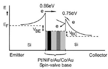
The schematic energy diagram
of the SVT showing the Si-Pt emitter and Si-Au collector Schottky barriers
and the spin-valve base. EF is the Fermi level, VBE is the base-emitter
bias, VBC is the base-collector bias.
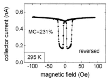
The magnetic field dependence
of collector current in the reverse mode of the SVT (IE =
2 mA, VBC = 0) showing a magnetocurrent of 231%.
The
SVT is based on spin-dependent transport of hot electrons rather than
electrons near the Fermi energy. The energy of the hot electrons is determined
by the Schottky barrier height at the emitter side of the device. The
injected electrons can only be collected if they have retained enough
energy to surmount the collector Schottky barrier, which is slightly lower
than the emitter barrier. Although large magnetocurrent effects (>300%)
and high field sensitivities have been demonstrated at room temperature,
a small output current (~20 nA) limits the application potential of the
SVT. The reason for the small output current is mostly the limited collection
efficiency due to the small difference between the two Schottky barrier
heights.
The IBM group [S. Van Dijken, X. Jiang and S.
S. P. Parkin, Phys. Rev. B 66, 094417 (2002)] presents the room temperature
operation of a magnetic tunneling transistor(MTT). The MTT consists of
a ferromagnetic emitter, a tunnel barrier, a single ultrathin FM base
layer, and a GaAs(111) collector. The spin-polarized electron current
that is injected from the emitter into the base is further spin filtered
by spindependent scattering in the FM base layer. As a consequence, the
collector current depends critically on the orientation of the magnetic
moment of the base with respect to that of the emitter. Output currents
larger than 1 mA and magnetocurrent changes of 64% are obtained at a bias
voltage of 1.4 V across the tunnel barrier. The output current of this
single base layer MTT is 2¡V3 orders of magnitude larger than the output
current previously reported for SVT.
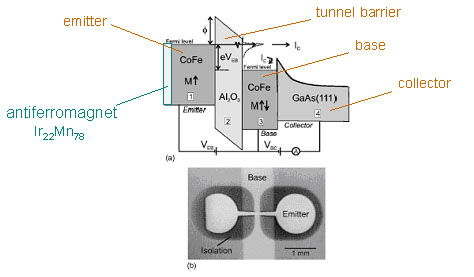
(a) Schematic energy diagram
of a MTT. Region 1 is the emitter, region 2 is the Al2O3
tunnel barrier, and region 3 is the base. The collector is the GaAs(111)
substrate (region 4). (b) Photo showing the active area of a MTT.
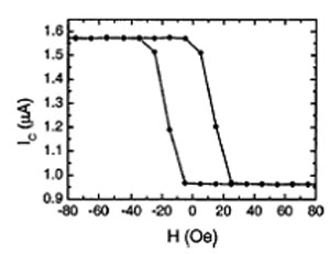
Collector current of an
MTT as a function of the applied magnetic field showing a magnetocurrent
of 64 ¢M. The emitter/ base bias voltage is 1.4 V.
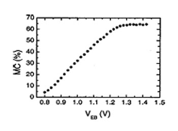
The emitter/ base bias
dependence of the magnetocurrent at room temperature.
There
are some main research subjects for spin valve transistor: (a) How to
make the transfer ratio of the device higher? (b) How to improve the output
current and characterize the noise behavior? Many researches have been
focused on the output current level and noise sources. Further improvements
are still required.
The basic concept of the SVT has also led to the
development of a number of related devices, such as the MTT. The variable
of the hot-electron energy gives possibilities of spectroscopic studies,
while enhanced base transmission is anticipated. Moreover, it has been
realized that hot-electron spin filtering may have some attractive features
for spin-injection into a semiconductor, in particular the ability to
reach a spin polarization near 100% with conventional ferromagnets.
Another interesting research is the study of hot-electron spin-transport
in half-metallic ferromagnets oxides. Such materials may also offer new
types of spintronic devices combining ferromagnets and semiconductors.
Spin-polarized
Field-effect Transistor
In 1990, Datta and Das proposed a design for a
spin-polarized field-effect transistor, or spin FET [S. Datta and B. Das,
Appl. Phys. Lett. 56, 665 (1990)]. This idea is at first glance much like
a conventional FET. In a conventional FET, a narrow semiconductor channel
runs between two electrodes named the source and drain. When voltage is
applied to the gate electrode, which is above the channel, the resulting
electric field drives electrons out of the channel (for instance), turning
the channel into an insulator.
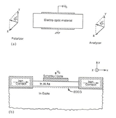
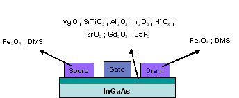
¡]a¡^ Electro-optic modulator¡]b¡^ proposed electron wave along of the electro-optic modulator.
The
spin FET has ferromagnetic source and drain so that the current flowing
into the channel is spin-polarized. The current¡Vcarrying medium would
be a channel layer formed at the heterojunction between InAlAs and InGaAs.
The two-dimensional electron gas (2DEG) in that layer would provide a
very high mobility channel, free of spin-flip scattering events. When
a voltage is applied to the gate, the current modulation in the proposed
structure arises from spin precession due to the strong spin-orbital coupling
in narrow-gap semiconductors (InGaAs, for this system).
The modulation of current can be expected by controlling the alignment
of a carrier¡¦s spin with respect to the magnetization vector in the collector
electrode. The gate electrode on the top of the device can be used for
controlling the spin-orbit interaction if the interaction is dependent
on the interface electric field. Such that one of the key ideas of the
above device is that how the spin-orbital interaction in a narrow gap
semiconductor and the electric field causes the precession of the spin
carriers.
There are some main research subjects for realizing
a spin FET: (a) How to modify the strength of spin-orbit coupling by the
gate voltage? (b) What is an efficient way to inject spin-polarized currents,
or spin currents, into a semiconductor? (c) What is the transport behavior
of spin polarized electrons in 2DEG? How long can a spin current retain
its polarization in a semiconductor? (d) What happens to spin currents
at boundaries between different semiconductors? (e) Can we make semiconductors
that are ferromagnetic at room temperature? The devices should be able
to operate at room temperature.
The (a) has been verified [Junsaku Nitta et al.,
Phys. Rev. Lett. 78, 1335(1997)]. The second problem remains unclear,
although there are some papers describing the success of spin injection
to semiconductors. With respect to the (c), it has been observed that
the spin diffusion length in the 2DEG is in the order of £gm, and an electric
field could push the spin polarized carriers over distance in the order
of 100£gm. [D. Hagelle et al., Appl. Phys. Lett. 73, 1580(1998)20]
A spin FET would have several advantages over
a conventional FET. To flip an electron's spin takes much less energy
and can be done much faster than pushing an electron out of the channel.
However, no one has succeeded in making a working prototype of the Datta-Das
spin FET because of difficulties in efficiently injecting spin currents
from a ferromagnetic metal into a semiconductor. Such that, the spin-injection
is one of the most important subjects that scientist interest in. Since
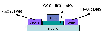
Fe3O4 can be epitaxially grown on GaAs, we will
combine Fe3O4 and III-V-based DMS to form spin MOSFET.
Schmidt et al. ( Phys. Rev. B62, R4790 (2000) )revealed that the basic obstacle for spin injection from a FM metal emitter into a semiconductor originates from the conductivity mismatch between these materials. E. I. Rashba ( Phys. Rev. B62, R16267 (2000) ) indicated that the spin injection coefficient controlled by the element of a FM-T-N-junction having the largest effective resistance. We plan to fabricate Fe3O4 based TMR junctions and investigate how the interfacial chemical state and the spin polarization affect the spin transport. Finally, we will use Fe3O4 and DMS to form spin transister.