„«¬ã
¨s ¤è ¦V
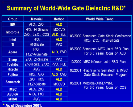
Atomic Layer deposition (ALD) as a technique which allows film deposition with monolayer precision has matured substantially and is now being introduced into semiconductor processing. Key ALD application include the deposition of high-k dielectrics, metal electrodes, barriers, and spacers.
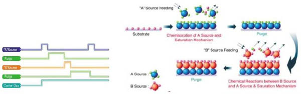
ALD is based on the sequential deposition of individual monolayer or fractions of a monolayer in a well controlled manner. The growth surface is alternately exposed to only one of two complementary chemical environments, i.e. individual precursors are supplied to the reactor one at a time. Exposure steps are separated by inert gas purge or pump-down steps in order to remove any residual chemically active source gas or by-products before another precursor is introduced into the reactor.
Thus,
ALD consists of a repetition of individual growth cycles. Each cycle is
made up of a typical sequence :
Flow of precursor A ¡÷ Purge ¡÷ Flow of precursor B ¡÷ Purge. During each
exposure step, precursor molecules react with the surface until all available
surface sites are saturated.
The advantages of ALD film
- Film thickness is given by the numbers of deposition cycle
- 100% step coverage even at high aspect ratios
- Lower deposition temperatures
- Films are very uniform, smooth