„«¬ă
¨s ¤č ¦V
| Research Interest | ||||
„«¬ă
¨s ¤č ¦V |
||||
| MBE Growth Process | ||||
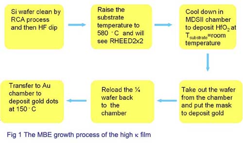
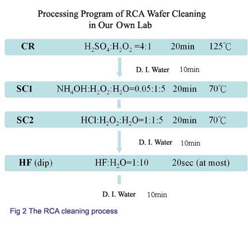
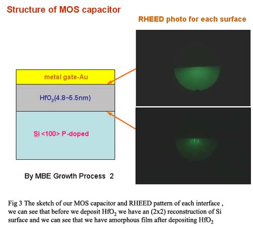
| „« We had used the molecular beam epitaxy method to grow the HfO2 dielectrics. By this approach We expect to achieve the atomically abrupt interfaces of HfO2 on Si in the absence of formation of SiO2 or silicates. This is because our oxide films are deposited by e-beam evaporation from preconditioned oxide sources rather than evaporation of metal sources and oxidizing at the Si surface with an external oxygen source. Having an atomically abrupt and smooth interface without the formation of SiO2 and silicates is significant, because a tremendous thickness saving in the equivalent oxide thickness (EOT) will be achieved. | ||||
|
||||
|
||||
|
||||
|
||||
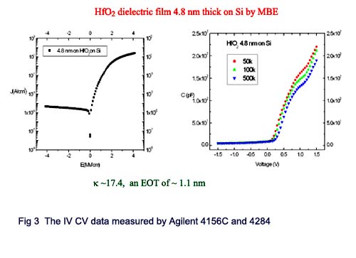
| Now we had successful improved our EOT to 1.1nm .We can see the Fig3 shown very low leakage current density 2.5x10⁻⁵ A/cm2 at 1 (MV/cm) with a dielectric constant of 17.4, and an EOT of 1.1 nm. Au dots of 0.1 mm diameters were evaporated as the metal gate electrodes. And the film thickness are measured by ellisometry. | ||||