


|
研究近況 |
||
|
Electronic versus Lattice Match for Metal-Semiconductor Epitaxial Growth: Pb on Ge(111) |
||
Reference 1. M. Upton, C. M. Wei, M. Y. Chou, T. Miller, and T.-C. Chiang, Phys. Rev. Lett. 933, 026802 (2004). 2. W. B. Jian, W. B. Su, C. S. Chang, and T. T. Tsong, Phys. Rev. Lett. 90, 196603 (2003). 3. M. Hupalo, V. Yeh, T. L. Chan, C. Z. Wang, K. M. Ho, and M. C. Tringides, Phys. Rev. B 711, 193408 (2005). 4 Phys. Rev. Lett. 933, 216804 (2004). 5. S.-J. Tang, Chang-Yeh Lee, Chien-Chung Huang, Tay-Rong Chang, Cheng-Maw Cheng, Ku-Ding Tsuei, H.-T. Jeng, V. Yeh, and Tai-Chang Chiang, Phys. Rev. Lett. 107, 066802 (2011) 6. S.-J. Tang, T. Miller, and T.-C. Chiang, Phys. Rev. Lett. 96, 036802 (2006). |
It has been a long-standing puzzle for years that metal films can grow smoothly on semiconductor surfaces, retaining its own lattice constant, in spite of large lattice mismatch [1, 2, 3, 4]. In the past, scientists have either overlooked the reason or naively assumed that the large lattice mismatch caused the metal films to be free-standing-film-like. In a recent Phys. Rev. Lett. paper [5], Shu-Jung Tang of TUNational Tsing Hua UniversityUT, TUHsinchuUT, TUTaiwanUT and co-workers reported the discovery of an important clue to this puzzle by investigating the system of Pb films on Ge(111). They showed that the growth of an incommensurate (1×1) parallel-epitaxy configuration is bound to another mysterious driving force for the epitaxial growth: electronic match. The perfect electronic match would cause the maximum hybridization between the quantum-well states (QWS) of the metal films and band edges of the semiconductor substrate so as to reduce the energy of the system.
Low energy
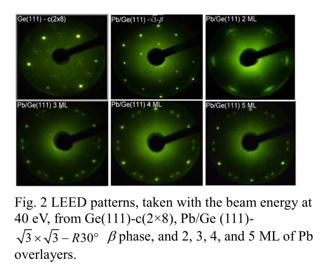
electron diffraction (LEED) measurements reveal the film growth orientation
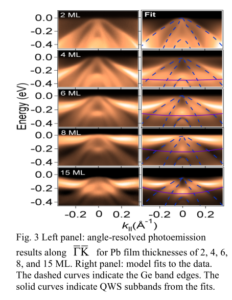
(Fig.2). Patterns from the bare Ge(111)-c(2×8) and the Pb/Ge(111) - The data at higher coverages (4-15 ML) in Fig. 4 are quite different; an Anderson model involving a hybridization interaction of the discrete Pb QWS subbands and the Ge states [5] is used to construct a model spectral function. The solid purple curve shows  ,
the dispersion of the "bare" QWS subband. ,
the dispersion of the "bare" QWS subband.
Two competing factors are at play: one is the interfacial energy, which is
independent of the film thickness and favors the The general understanding established in Tang, et al. [5], is important for devising strategies for smooth film growth with prescribed configurations – a key issue relevant to thin film electronics. |
|
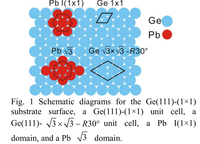
 unit
cell become well matched (Fig. 1).
unit
cell become well matched (Fig. 1).  -
-
 -
- pattern is suppressed. An attenuated Ge(111)-(1×1) substrate pattern remains and is
accompanied by six short arcs with the same orientation but farther out. The
radius of the arcs indicates an I(1×1) Pb overlayer. Also evident in the data is
the emergence of
pattern is suppressed. An attenuated Ge(111)-(1×1) substrate pattern remains and is
accompanied by six short arcs with the same orientation but farther out. The
radius of the arcs indicates an I(1×1) Pb overlayer. Also evident in the data is
the emergence of  domains
at 3 ML which eventually dominates at higher Pb coverages . Angle-resolved
photoemission mapping of Pb overlayers of thicknesses 2, 4, 6, 8, and 15 ML
along the
domains
at 3 ML which eventually dominates at higher Pb coverages . Angle-resolved
photoemission mapping of Pb overlayers of thicknesses 2, 4, 6, 8, and 15 ML
along the  direction
yield spectral functions shown in Fig. 3. At 2 ML, the results closely resemble
the k-resolved one-dimensional density of states of the Ge bulk band
structure because of a strong hybridization of the Pb and Ge states and the
large contribution from the Ge states within the photoemission probing depth
[6].
direction
yield spectral functions shown in Fig. 3. At 2 ML, the results closely resemble
the k-resolved one-dimensional density of states of the Ge bulk band
structure because of a strong hybridization of the Pb and Ge states and the
large contribution from the Ge states within the photoemission probing depth
[6].  lattice-matched configuration, and the other is the
electronic energy associated with quantum confinement, which diminishes as
1/N and also depends on the degree of electronic hybridization across the
Pb-Ge interface. A strong hybridization as a result of electronic match
minimizes the effects of confinement, leading to a lower system energy. The
authors convincingly argue that the I(1×1) configuration presents a much better
electronic match than the
lattice-matched configuration, and the other is the
electronic energy associated with quantum confinement, which diminishes as
1/N and also depends on the degree of electronic hybridization across the
Pb-Ge interface. A strong hybridization as a result of electronic match
minimizes the effects of confinement, leading to a lower system energy. The
authors convincingly argue that the I(1×1) configuration presents a much better
electronic match than the  configuration based on general symmetry considerations.
Thus, the I(1×1) configuration is preferred at small thicknesses for
Pb/Ge(111).
configuration based on general symmetry considerations.
Thus, the I(1×1) configuration is preferred at small thicknesses for
Pb/Ge(111).
|
|
|
|
|
 標題
標題

Copyright (c) 2010 Photoemission Lab. All rights reserved.